Senior Patent Research Analyst, 3AIP Services Pvt. Ltd., Zirakpur, Punjab
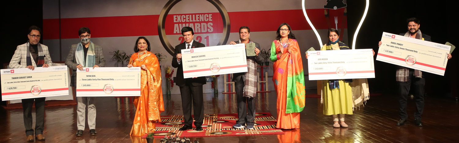
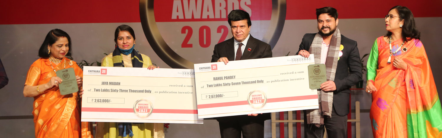
I am glad that I got the opportunity to work under the guidance of Dr. Rajnish Sharma, Dr. Rahul Pandey, Dr. Jaya Madan, Dr. Kulbhushan Sharma and other members of the VLSI team. I have total of Eight publications in the field of analog circuit design and solar cell technology. I can't be thankful enough as their technical expertise and support made me advance my career in the research field.

Junior Research Fellow (JRF) from Department of Electrical and Electronics Engineering at University of Petroleum and Energy Studies,
The VLSI center of excellence has acted like a base to me. I have learnt about the research techniques and base of research from there only. The guidance of the members helped me a lot in deep learning and for further growth. I have published 6 research papers in international Journals and Cconferences.
JRF at IIIT Delhi
The three Years at Chitkara University have been a brilliant experience, with exposure in both theory and practical domains. The VLSI COE provides me with a great opportunity to explore myself with great guidance. My research expertise is in the design and simulation of thin-film solar cells. I worked on Perovskite, CZTSSe, SnS, and tandem solar cells. I have published 6 research papers in international Journals and Conferences. I also have 4 patents with my name.
ME Research Fellow
Qualification:B.E. (ECE)
Topic of research: Design and Simulations of Lead free and low lead content-based perovskite solar cell
Email Id: sakshi.sharma@chitkara.edu.in
Post Silicon Validation Engineer at NXP Semiconductors, Bengaluru, India
Testimonial: I took VLSI as the core subject during my journey of ECE (2018-2022) as it made me curious. While exploring various aspects of this field, I dived into Analog Layout Design which was also the part of our course, I even did my major project based on the same and with the wonderful direction that our professor Dr. Kulbhushan Sharma gave me, I was able to document the research paper about my project (“A Low-Noise High-Gain Recycling Folded Cascode Operational Transconductance Amplifier Based on Gate Driven and Quasi-Floating Bulk Technique”) which was then published by Journal of Circuits, Systems, and Computers, World Scientific on 15th November,2021. Further I got the opportunity to work with NXP Semiconductors and now I am working on the post silicon validation of various Analog Mixed Signals IP blocks, learning and improving with each new step.

Verification engineer in NXP Semiconductors, Bangalore, India.
The lab is the place where I learn how much intresting VLSI domain can be. While working under effective guidance Dr. Kulbhushan Sharma and Mrs. Preeti Sharma and learning how to make layout of amplifier was one of the best experience of my graduation period. I love working in the lab so much that I sometimes forgot time and immersed in making the layout. It was a great learning experience for me and I hope everyone enjoy it as much as I do.
Verification engineer in NXP Semiconductors, Bangalore, India.
Sonal Kapila, 2018-2022 batch, E&CE currently working as a verification Engineer at NXP semiconductors, Bangalore. I am a VLSI enthusiast and want to explore all its domains. My major project includes Analog Layout design of ultra-low power signal conditioning system which got published in Journal of Micromechanics and Microengineering 31 (12), 124005 under guidance of Dr. Kulbhushan Sharma.
Technical Intern at Luminous Power Technologies Baddi, HP. Placed in SIEMENS INDIA LTD.
I was at stage zero when I start working in the VLSI domain but gradually I develop interest in this field. Thanks to Dr. Kulbhushan Sharma and Mrs. Preeti Sharma of VLSI department for providing skill to implement layout of low voltage operational transconductance amplifier. Every time when I work on CADENCE it motivates me to make something big along with the utmost precision. It’s an everlasting motivation gained from VLSI lab in this journey of knowledge enhancement.